ENG | Arduino: MOSFETs
Explore the principles and practical usage of P-channel MOSFETs as high-side switches. Learn about the importance of threshold voltage, gate control, and circuit implementations using an Arduino. Understand the considerations for selecting the right MOSFET and including a gate resistor for optimal performance.
This article is work in progress. Likely will be till May (2025?).
Motivation to use P type logic level MOSFET as a voltage controlled switch or latch are the following applications:
- to shut down some power consuming device (e.g. SD card reader with inefficient voltage regulator)
- to shut down microcontroller when battery is low and to prevent it from turning on again
- reverse polarity protection without voltage drop of diode
Take this article as something that I self-learned and do not fully trust it.
What is MOSFET
A MOSFET is a type of field-effect transistor (MOS stands for metal oxide semiconductor) that is widely used for amplifying or switching electronic signals. It consists of a source, drain, and a gate terminal. The gate is separated from the body of the transistor by a thin insulating layer, typically made of silicon dioxide.
The operation of a MOSFET is based on the principle of the field effect. When a charge is applied to the gate terminal, it creates an electric field that controls the flow of charge carriers (electrons or holes) between the source and drain terminals. This allows the MOSFET to act as an electrically controlled switch or a latch.
TODO: image
While the gate itself is insulated and does not draw a continuous current, it can draw a significant amount of current during the charging and discharging phases, especially when switching at high frequencies. This is because the gate acts as a capacitor that needs to be charged or discharged to turn the MOSFET on or off.
In applications where fast switching times are important, a dedicated MOSFET driver circuit may be necessary. The driver circuit ensures that the gate is charged and discharged quickly and properly, minimizing unwanted transients and ensuring reliable switching behavior.
MOSFET vs bipolar transistor vs IGBT
| Bipolar | MOSFET | IGBT | |
|---|---|---|---|
| Operation speed | Slow | Fast | Slow/Moderate |
| Drive power | High | Low | Low |
| Large current capacity | Excellent | Poor | Excellent |
- Bipolar transistors: Suitable for low-power applications, driven by current, resulting in higher drive losses.
- MOSFETs: Driven by voltage, low drive losses, suitable for high-frequency applications.
- IGBTs: Low drive losses, suitable for high-power applications with moderate switching speeds.
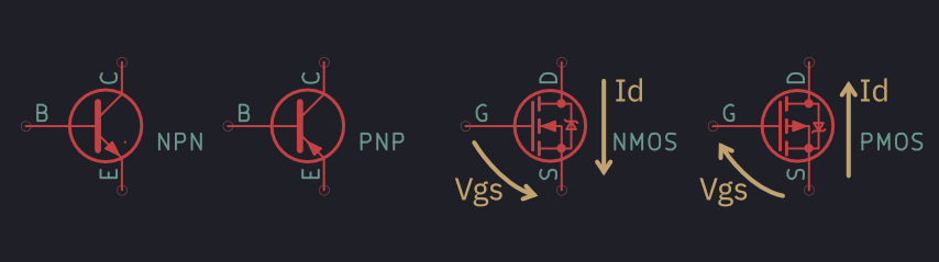 Electronic symbols of different transistors
P-MOSFET vs N-MOSFET
- N-Channel MOSFETs: Turn on when the gate voltage is higher than the source voltage.
- P-Channel MOSFETs: Turn on when the source voltage is higher than the gate voltage.
N-Channel MOSFETs generally have better performance (lower $R_{DS}(on)$ at the same gate capacitance) compared to P-Channel MOSFETs, resulting in faster switching and lower power losses in the conductive state. The performance of a MOSFET is determined by its input capacitance ($C_{iss}$, which is a combination of the gate-drain and gate-source capacitances) and its on-resistance ($R_{DS}(on)$).
For larger current handling capabilities (and lower $R_{DS}(on)$), MOSFETs have a larger active area, which proportionally increases the gate capacitance. GaN FETs, used in compact, modern, and efficient phone chargers and notebook power supplies, have exceptionally low gate charge and are suitable for fast switching applications.
MOSFET’s parameters
For our applications, where we do not need high voltage, current, or switching speed, the following parameters are important:
- $V_{GS}(th)$: The voltage between the gate and source terminals that is required to fully open the transistor. For 3-3.3V logic and switching off a battery, this value should be lower than 2.5V - and less is more.
- $R_{DS}(on)$: The resistance between the source and drain terminals when the MOSFET is fully on. Typically, P-channel MOSFETs tend to have higher on-resistance compared to N-channel MOSFETs, especially those with low $V_{GS}(th)$ values.
- $I_{D}$ (Drain Current): The maximum continuous drain current that the MOSFET can handle without exceeding its safe operating area.
Examples of MOSFETs I have at home:
| Type | $V_{GS}(th)$ | $R_{DS}(on)$ | Package | Pins | Note |
|---|---|---|---|---|---|
| IRF9Z34N | -2V to -4V | 0.1Ω | TO220 | GDS | Id @ Vgs(th) = 250μA |
| TP0606N3-G | -2.4V max | 5Ω | TO92 | SGD | Id @ Vgs(th) = 1mA, Rds(on) @ Vgs=-5V |
| LP0701 | -0.5 to 1V, -0.7V typ, | 1.7Ω | TO92 | SGD | Id @ Vgs(th) = 1mA, Rds(on) @ Vgs=-3V |
P-MOSFET as a high-side switch
This paragraph highlights the importance of understanding $V_{GS}(th)$ parameter and a pull-up resistor
A high-side switch is a configuration where the MOSFET is placed between the load and the positive supply voltage (VCC). This > arrangement allows the MOSFET to control the power delivery to the load by acting as a switch. Some benefits of a high-side switch include:
- Allowing the load to be fully disconnected from the power supply, reducing potential leakage currents.
- Providing a more straightforward implementation for applications where the load is connected to ground or requires a common ground reference.
A P-MOSFET conducts when the gate is grounded (or connected to a lower potential than the source), and it shuts down when the gate voltage is approaching source voltage and difference is below $V_{GS}(th)$. When the gate is floating (not connected to any potential), its state is undefined, and it can exhibit unexpected behavior:
- When you expect it to conduct, it won’t conduct.
- When you expect it not to conduct, it may be partially on or “half-open.”
- When you touch it, it can randomly change state and stay in that state.
- The behavior can be inconsistent and may depend on factors like the power source (e.g., a phone charger or a notebook battery).
Messing with MOSFET’s floating gate
To prevent the MOSFET from conducting when it should be off (default state), we need to connect the gate to the positive supply voltage (VCC) through a high-resistance pull-up resistor, typically around 100kΩ-1MΩ.
Now I can measure the current and it is … 3.3uA. Wait, what?
When I leave the gate floating, it’s 3mA … ok it’s in undefined state. When gate resistor is changed from 1M to 100k, current is 6μA. Doesn’t make any sense 🤯.
It’s very weird, cause zero drain current should be below 10μA while switching 60V rather than 5V. It also depends on temperature, but specifications are for 25C. Is it damaged? Is there something in datasheet I overlooked? I don’t know ¯\_(ツ)_/¯.
The next day I realized that it does matter if the gate pin is connected before or after the multimeter which measures current and I also measurent 18μA. Ok, Heisenbugs obviously exist in electronics design too.
We can try to upload blink demo to Arduino and connect gate to D13 pin.
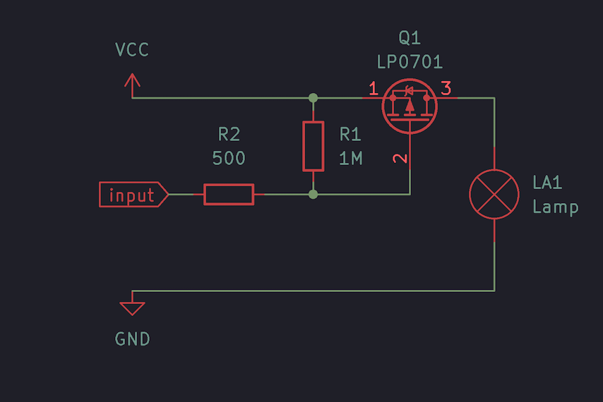
MOSFET switch. 500Ω resistor is ommited. It should limit current from pin 13 below 10mA
This works as expected. When pin state is low, LED is off, but MOSFET turns light bulb on.
When we want to reverse this behaviour, we can use transistor (i guess any NPN is fine) and connect gate to ground when pin state is high to make it conduct.
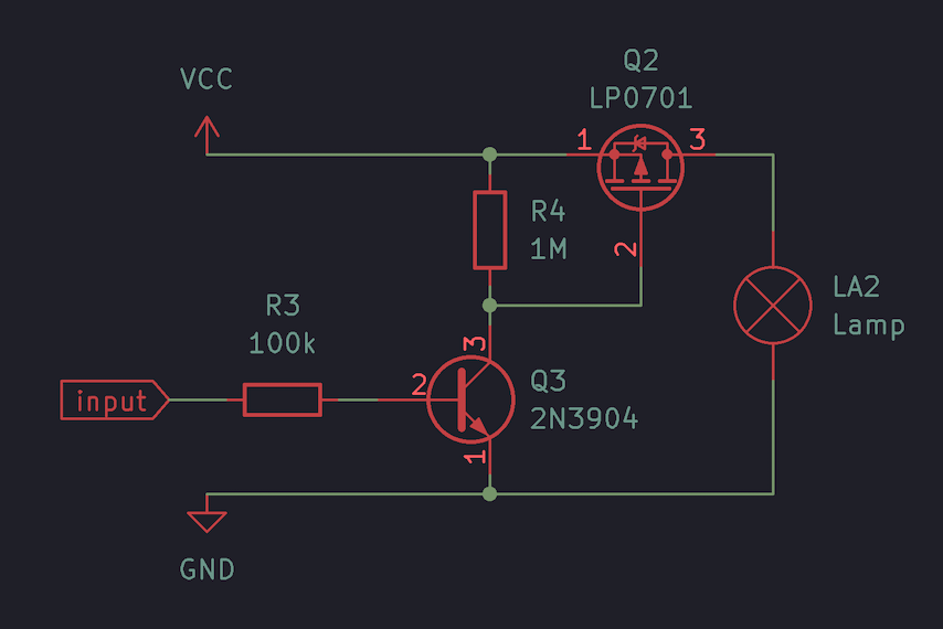
The later version with transistor added and switching 3.3V. White wire goes from pin D13 to gate of transistor via 100k resistor. Yellow wire goes from collector to gate of P-MOSFET.
I used this switching circuit years ago to shut down power to SD Card adapter due to inefficient voltage regulator, other option is to remove it completely and use more efficient one. I measured that SD card adapter uses cca 2,23mA without card and 2,32mA with card inserted and high tens of miliamps during writes.
High side switch was used because I wanted all pins going to SD card grounded when it’s off.
It is generally recommended (best practice) to include a resistor in series with the gate of the MOSFET, even when using an NPN transistor as a driver.
- This resistor helps limit the gate current and prevents potential damage to the MOSFET or the transistor driver during switching transitions.
- When the gate capacitance is charged or discharged too quickly, it can lead to oscillations or ringing due to the parasitic inductances in the circuit. The gate resistor helps dampen these oscillations by slowing down the charging/discharging of the gate capacitance.
- Controlling switching times: The gate resistor, in combination with the gate capacitance, forms an RC time constant that determines the rise and fall times of the gate voltage during switching transitions. This can help control and make the switching times more predictable. However, in many low-frequency switching applications, such as the P-MOSFET switch described, the oscillations and switching times may not be critical concerns. In these cases, it is common practice to omit the gate resistor, especially when the gate is driven by a low-impedance source (e.g., a microcontroller pin or a transistor).
Further exploration
- Low side switch using N-MOSFET
- Reverse polarity protection
- Find some logic level mosfets in reasonable package
Summary
In this article, we explored the principles and practical usage of P-channel MOSFETs as high-side switches. We covered the following key points:
- Understanding the importance of the threshold voltage ($V_{GS}(th)$) parameter and the need for a pull-up resistor to properly control the gate voltage.
- The behavior of a P-MOSFET when the gate is floating, and the potential for undefined or undesirable states.
- Selecting the appropriate MOSFET based on its $V_{GS}(th)$ and $R_{DS}(on)$ values for a given application.
- Practical circuit implementations using an Arduino to control a P-MOSFET switch, with and without an NPN transistor as a gate driver.
- Considerations for including a gate resistor to control switching times and prevent oscillations, depending on the application requirements. By understanding the fundamental principles and characteristics of P-MOSFET switches, you can effectively design and implement circuits for various low-frequency switching applications, such as controlling power to loads or managing power consumption in battery-powered devices.
Resources
Article is partially based on old article from 2016-06-01, tested from scratch and improved by Claude Sonnet AI.